Digital Logic — Cram
Every digital logic question on one page. Back to index
Basic gates from a 2:1 mux and from NAND
Question
Build NOT, AND, OR, XOR, NAND and NOR using only 2:1 multiplexers, and separately using only NAND gates. Why is a 2:1 mux functionally complete, and what is the minimum NAND count for XOR?
Key idea
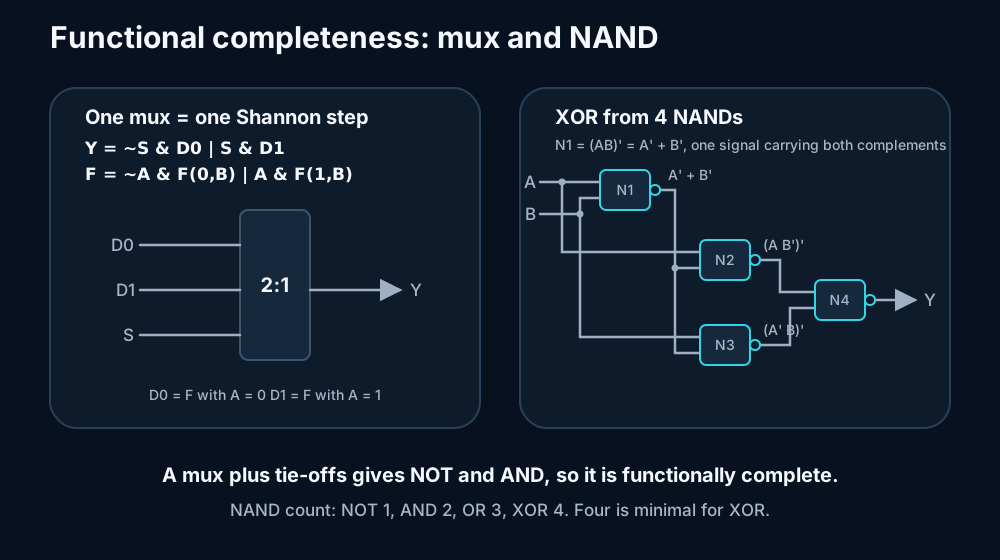
A 2:1 mux computes Y = ~S & D0 | S & D1, which is exactly Shannon’s expansion F = ~A & F(0,B) | A & F(1,B). So drive S with A and the data inputs are just F with A forced to 0 and to 1 — read off, never guess. For NAND, massage the expression until its outermost operation is a complemented product, because that shape is a NAND.
Answer
From 2:1 muxes
With Y = S ? D1 : D0, substitute A = 0 and A = 1 into the target function and read off the cofactors:
| Gate | S | D0 = F(0,B) | D1 = F(1,B) | muxes |
|---|---|---|---|---|
| NOT | A | 1 | 0 | 1 |
| AND | A | 0 | B | 1 |
| OR | A | B | 1 | 1 |
| NAND | A | 1 | B’ | 2 |
| NOR | A | B’ | 0 | 2 |
| XOR | A | B | B’ | 2 |
The split is entirely explained by the cofactor column. The cheap three need only 0, 1, or the bare wire B — all free. The expensive three need B', a complement, which is not a free signal and costs the second mux. Swapping which variable drives the select does not rescue you: expand NAND on B instead and the cofactors are 1 and A', still a complement.
Generalising: with S = A and each data input drawn from {0, 1, B}, one mux realises 9 of the 16 two-variable functions. The other 7 all need a complemented input. If both polarities are already available — common in real silicon, since a flop gives you Q and Q' — all six collapse to a single mux.
From NAND gates
| Gate | Construction | NANDs |
|---|---|---|
| NOT | NAND(A,A), since A·A = A |
1 |
| AND | NAND(A,B) then invert |
2 |
| OR | NAND(A', B') = (A'·B')' = A + B by De Morgan |
3 |
| XOR | see below | 4 |
| NOR | OR then invert | 4 |
The minimal 4-gate XOR, where the trick is that N1 is a shared term used twice:
| Gate | Expression | Simplifies to | Why |
|---|---|---|---|
| N1 | NAND(A,B) |
A' + B' |
De Morgan |
| N2 | NAND(A, N1) |
(A·B')' |
A(A'+B') = 0 + A·B' |
| N3 | NAND(B, N1) |
(A'·B)' |
B(A'+B') = A'B + 0 |
| N4 | NAND(N2,N3) |
A·B' + A'·B |
De Morgan on the output |
N1 = (AB)' = A' + B' is one signal carrying both complements at once. ANDing it with A annihilates the A' term and leaves A·B'; by symmetry B leaves A'B. The naive sum-of-products route costs 5 because it builds A' and B' as two separate single-use signals; the fully literal AND-OR translation costs 9.
Four is the proven minimum. By duality, swapping every NAND for a NOR in that table yields XNOR in 4 NORs.
Why a mux is functionally complete
Two arguments, both worth having.
Reduction. One mux gives NOT (D0=1, D1=0) and one gives AND (D0=0, D1=B). {NOT, AND} is a complete basis, therefore the mux is complete. Three lines.
Structural. One mux is one Shannon expansion step, consuming one variable and leaving two functions of n-1 variables on its data inputs. Recurse: after n levels the data inputs are functions of zero variables, i.e. constants. So any n-input function is a binary mux tree of depth n with 2^n - 1 muxes and 2^n constant leaves — which is precisely an FPGA lookup table. A 4-LUT is a 16:1 mux whose data inputs are SRAM cells holding the truth table.
Cost
Mux counts: NOT 1, AND 1, OR 1, NAND 2, NOR 2, XOR 2. NAND counts: NOT 1, AND 2, OR 3, XOR 4, NOR 4. An n-input function needs 2^n - 1 muxes as a tree.
In CMOS a NAND is 4 transistors while an AND is 6 (NAND plus inverter), which is why NAND-based logic is the cheap default.
Gotchas
- The completeness proof requires tie-offs to 0 and 1. A 2:1 mux with all three inputs driven by variables is not functionally complete: feed all ones and you get 1, feed all zeros and you get 0, so it is both 0-preserving and 1-preserving, and no circuit of such gates can ever produce NOT. Say “complete over the basis including constants” and you are answering above level.
- In the 4-NAND XOR,
N2andN3are the complements of the product terms, not the products. That is the point — the final NAND expands by De Morgan toN2' + N3', which un-inverts and ORs them in one gate. “Isn’t N2 inverted?” is the standard follow-up. - Derive cofactors by substitution, not intuition. Guessing is where people lose XOR and NOR under pressure.
- “Muxes can build any gate, and FPGAs use muxes” restates the claim rather than proving it. The FPGA fact is a consequence of Shannon completeness, not evidence for it.
Follow-ups
- Build a 4:1 mux from 2:1 muxes. Three of them, two levels — one Shannon step per select bit.
- Is NOR functionally complete? Yes, dual argument: NOR gives NOT and OR.
- Why are LUTs mux trees? The recursion above. You change the function by rewriting the SRAM leaves rather than rewiring anything.
- Cheapest XOR in CMOS? Not the 4-NAND version — a transmission-gate XOR is 6 transistors.
- 2:1 mux from NANDs? Four, same count as XOR.
FSM to check divisibility by 5
Question
Design an FSM that checks whether a number is divisible by 5. Bits arrive serially, one per clock, MSB first. Assert an output when the number received so far is divisible by 5. How many states, why, and what are the transitions?
Key idea
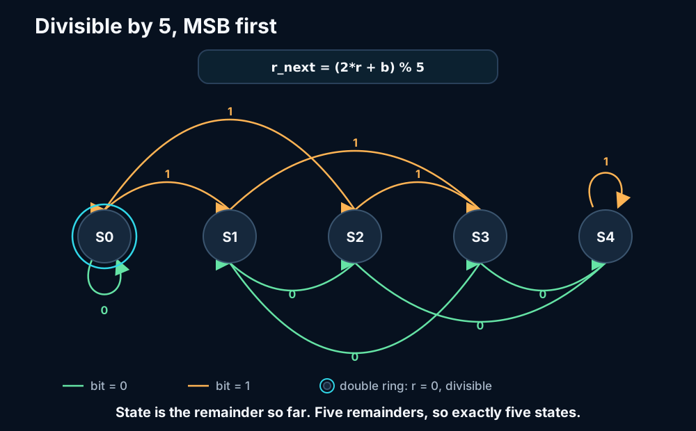
Appending a bit MSB-first turns the value N into 2*N + b, and divisibility only depends on N % 5, so a state need hold nothing but the remainder. Five possible remainders means exactly five states, with r_next = (2*r + b) % 5.
Answer
This is not a sequence detector. It is arithmetic: each new bit shifts the accumulated value left and lands in the ones place, so N -> 2*N + b. Since N is unbounded you cannot store it, but you do not need to — only N % 5 matters, and modular arithmetic distributes over both the multiply and the add.
Let state Sr mean “the value so far leaves remainder r”. Reset to S0.
| State | bit 0 | bit 1 |
|---|---|---|
| S0 | S0 | S1 |
| S1 | S2 | S3 |
| S2 | S4 | S0 |
| S3 | S1 | S2 |
| S4 | S3 | S4 |
module div5 (input logic clk, rst, inp, output logic oup);
  typedef enum logic [2:0] {S0, S1, S2, S3, S4} state_t;
  state_t state;
  logic   valid;

  always_ff @(posedge clk) begin
    if (rst) begin
      state <= S0;
      valid <= 1'b0;
    end
    else begin
      valid <= 1'b1;
      case (state)
        S0:      state <= inp ? S1 : S0;
        S1:      state <= inp ? S3 : S2;
        S2:      state <= inp ? S0 : S4;
        S3:      state <= inp ? S2 : S1;
        S4:      state <= inp ? S4 : S3;
        default: state <= S0;
      endcase
    end
  end

  assign oup = valid && (state == S0);
endmodule
Moore or Mealy is a design choice, not a property of the problem. oup = (state == S0) is Moore: registered, glitch-free, but reporting on bits through the previous cycle. oup = (next_state == S0) is Mealy: valid in the same cycle the bit arrives, matching the wording of the question, at the cost of a combinational path from inp to the output. State and transition logic are identical either way.
The arithmetic form generalises and is cheaper than the case statement:
  logic [3:0] sum;
  assign sum = {state, 1'b0} + inp;   // 2*r + b, at most 9
  always_ff @(posedge clk)
    if (rst) state <= '0;
    else     state <= (sum >= 5) ? sum - 4'd5 : sum;
Cost
Five states, so 3 state bits. The arithmetic version is one 4-bit adder plus one mux — the compare and the subtract share an adder, since sum + 4'd11 produces sum - 5 in its low bits and the sum >= 5 condition in its carry-out.
Five is the true minimum: all five remainders are behaviourally distinguishable, so no two can be merged.
Gotchas
- Never write
% 5in RTL — a general modulo infers a divider. Because2*r + b <= 9 < 10, a single conditional subtract of 5 always suffices. - Always include a
defaultin the statecase. With 3 bits encoding 5 states, values 5 to 7 are unreachable in theory but leave the FSM with no assignment, so it holds its value forever. In simulationstateis3'bxxxbefore reset, matches nothing, and staysxindefinitely. S0means both “remainder 0” and “nothing received yet”, so a bare Moore output asserts out of reset and claims the empty stream is divisible. Qualify it with avalidbit.- Set that valid bit unconditionally (
valid <= 1'b1), not withvalid <= valid | inp. The latter tracks “have I seen a one”, so a stream of zeros never reports divisible — but zero is divisible by 5. - Verilog syntax traps that bite here:
if (rst) begin ... endneeds itsendbeforeelse, and with ANSI-style ports you must not re-declare the ports in the body. - Verify a trace against the arithmetic, not against your own table.
1010is 10, so the machine must finish inS0.
Follow-ups
- Bits arrive LSB first. Different machine, 20 states — see the LSB-first variant.
- Divisible by any N. Same skeleton with N states and
r_next = (2*r + b) % N. The single conditional subtract still works because2*r + b < 2*N. - Output the remainder instead of a flag. Already there: the state encoding is the remainder, so just expose it.
- Divisible by a power of two. Degenerate — inspect the low bits, no FSM needed.
- Divisible by 3.
r_next = (2*r + b) % 3, three states.
FSM to check divisibility by 5, LSB first
Question
Same divisibility-by-5 checker, but bits now arrive LSB first — on cycle k you receive the bit of weight 2^k. What replaces the 2*N + b relation, what must a state hold, and how many states do you need?
Key idea
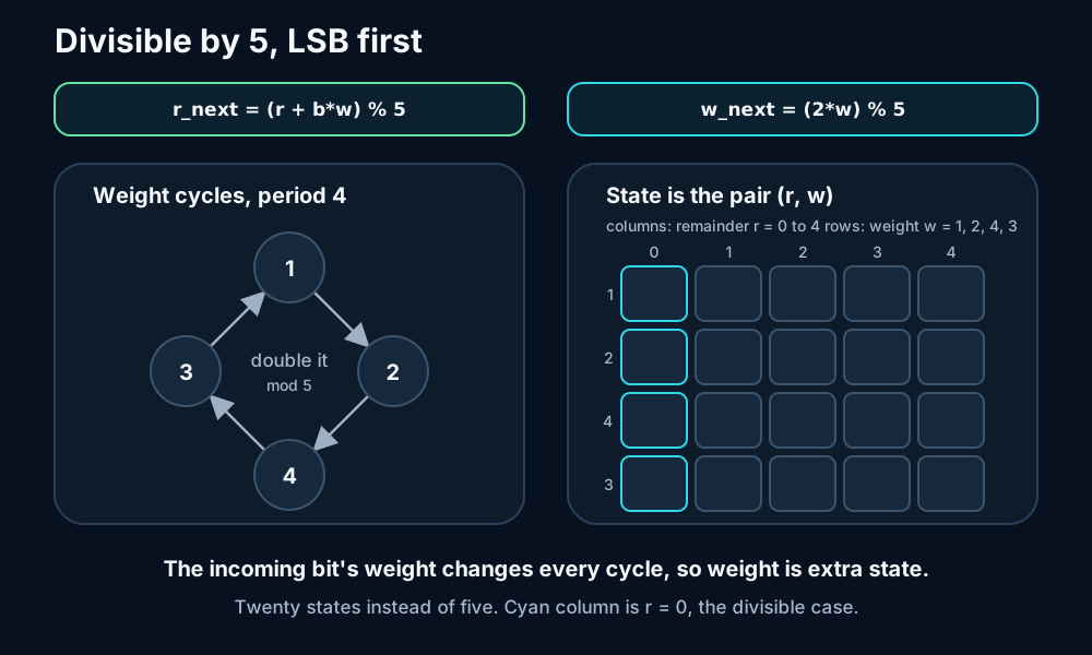
LSB-first, the bits you already hold never move; instead each new bit lands one position higher, so N -> N + b * 2^k. The remainder alone can no longer predict the next remainder because the bit’s weight depends on k, so state becomes the pair (remainder, weight) — and since 2^k % 5 has period 4, that is 5 * 4 = 20 states.
Answer
Compare what each direction needs in order to compute the next remainder:
| Arrival order | Value relation | Needs |
|---|---|---|
| MSB first | N -> 2*N + b |
remainder only, 5 states |
| LSB first | N -> N + b * 2^k |
remainder and weight, 20 states |
MSB-first the doubling acts on the accumulated value, which is computable from the remainder. LSB-first the scaling acts on the incoming bit, and the remainder tells you nothing about what the next bit is worth. Concretely: with r = 0 and an incoming 1, the new remainder is 1 at cycle 0, 2 at cycle 1, and 4 at cycle 2. Same remainder, same input, three outcomes — so they must be three distinct states.
The weight does not grow without bound, because only 2^k % 5 matters and that repeats:
2^0=1, 2^1=2, 2^2=4, 2^3=8->3, 2^4=16->1, ...
so w cycles 1, 2, 4, 3 with period 4, and each weight is the previous one doubled mod 5. That is one small register, not a lookup table.
module div5_lsb (input logic clk, rst, inp, output logic oup);
  logic [2:0] rem;    // N % 5:     0..4
  logic [2:0] wgt;    // 2^k % 5:   1, 2, 4, 3
  logic       valid;
  logic [3:0] acc, dbl;

  assign acc = rem + (inp ? wgt : 3'd0);   // at most 4 + 4 = 8
  assign dbl = {wgt, 1'b0};                // at most 2 * 4 = 8

  always_ff @(posedge clk) begin
    if (rst) begin
      rem <= 3'd0; wgt <= 3'd1; valid <= 1'b0;   // 2^0 % 5 = 1
    end
    else begin
      rem   <= (acc >= 5) ? acc - 4'd5 : acc;
      wgt   <= (dbl >= 5) ? dbl - 4'd5 : dbl;
      valid <= 1'b1;
    end
  end

  assign oup = valid && (rem == 3'd0);
endmodule
Trace 10, whose LSB-first bit stream is 0, 1, 0, 1 against weights 1, 2, 4, 3: the remainder goes 0, 0, 2, 2, (2+3)=5 -> 0. Ends at 0, and 10 is divisible by 5.
Cost
Twenty states, encoded as two registers rather than a flat 20-way case — rem is 3 bits and wgt is 3 bits, a product encoding. All 20 are reachable and pairwise distinguishable (two states with equal remainder but different weight diverge after a single 1), so 20 is minimal.
Each update is one 4-bit adder plus one mux. b * w is not a multiply: b is one bit, so it is a mux, or equivalently {3{inp}} & wgt.
Gotchas
N + 2*bis the wrong relation. The weight is not a constant 2, it is2^kand it grows every cycle.- Both updates stay in range for a single conditional subtract because
r + b*w <= 8and2*w <= 8, both under2 * 5 = 10. That is the general rule: one subtract suffices wheneverx < 2*M. wgtmust reset to 1, not 0. A zero weight is an absorbing state and the remainder would never change again.{wgt, 1'b0}for2*wstates the 4-bit width outright.wgt << 1works here only because of Verilog’s context-determined width rules for shifts — the concatenation removes the need to reason about it.- The 4-bit
accanddblassigned back into 3-bit registers is safe (post-subtract values are at most 4) but will raise a lint width warning. Slice explicitly if you want it clean.
Follow-ups
- Why is MSB first cheaper? General fact about serial arithmetic, not special to 5: appending at the LSB end is a fixed multiply-by-radix that folds into the state, while LSB-first forces you to carry positional weight.
- Four bits at a time. Since
2^4 = 16is congruent to 1 mod 5,N % 5equals the sum ofN’s hex digits mod 5 — accumulate nibbles with no weight tracking at all. This is the base-16 cousin of summing decimal digits to test divisibility by 9. - Divisibility by N, LSB first. State count is
Ntimes the multiplicative order of 2 modN. For 5 that order is 4; for 3 it is 2, giving only 6 states. - Why does the weight cycle at all? 2 is invertible mod 5, so repeated doubling walks a cyclic subgroup and must return to 1.